| CPC G06F 3/0608 (2013.01) [G06F 3/0658 (2013.01); G06F 3/0679 (2013.01); G06F 12/0246 (2013.01); G06F 13/4234 (2013.01); G06F 2212/1016 (2013.01); G06F 2212/1044 (2013.01); G06F 2212/177 (2013.01); G06F 2212/7202 (2013.01)] | 17 Claims |
|
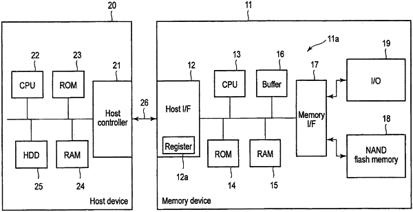
1. A memory device comprising:
a nonvolatile semiconductor memory having a plurality of physical storage areas that include an externally accessible user area, the user area being divided into a plurality of allocation units, the plurality of allocation units being divided into recording units; and
a control unit configured to control the nonvolatile semiconductor memory, wherein the control unit is configured to:
receive one or more control commands to designate a sequential write area for writing data;
assign, as the sequential write area, an allocation unit, of the plurality of allocation units, represented by an address of the one or more control commands;
receive one or more write commands, wherein:
the one or more write commands indicate access to an area, in the sequential write area, that has not been written;
a data length, indicated by the one or more write commands, is equivalent to one or more recording units; and
a data write location, indicated by the one or more write commands, is on a boundary of a recording unit; and
write data, associated with the one or more write commands, at an average speed that satisfies a write performance index.
|