| CPC G06F 3/0418 (2013.01) [G06F 3/0445 (2019.05); G06F 3/0448 (2019.05); G06F 2203/04107 (2013.01); G06F 2203/04111 (2013.01)] | 27 Claims |

|
1. An electronic device comprising:
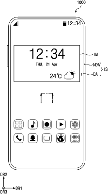
a display layer including a display region in which an image is displayed and a peripheral region adjacent to the display region; and
a sensor layer disposed on the display layer,
wherein the sensor layer includes:
a plurality of first electrodes arranged in a first direction;
a plurality of second electrodes arranged in a second direction crossing the first direction and crossing the plurality of first electrodes;
a plurality of first trace lines electrically connected with the plurality of first electrodes, respectively; and
a plurality of second trace lines electrically connected with the plurality of second electrodes, respectively,
wherein the plurality of first electrodes and the plurality of first trace lines are connected through a plurality of first contacts, respectively, and the plurality of second electrodes and the plurality of second trace lines are connected through a plurality of second contacts, respectively, and
wherein the plurality of first contacts and the plurality of second contacts overlap the display region.
|