| CPC G06F 3/04164 (2019.05) [G06F 3/044 (2013.01); G06F 3/0443 (2019.05); H10K 59/131 (2023.02); H10K 59/40 (2023.02); H10K 59/873 (2023.02); G06F 2203/04107 (2013.01)] | 16 Claims |

|
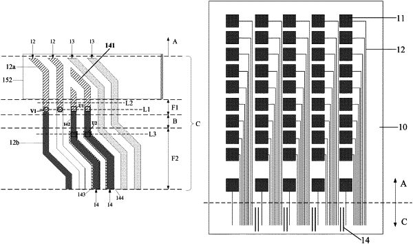
1. A display panel, comprising: a display area and a peripheral area positioned on at least one side of the display area; wherein
the display panel further comprises:
a substrate;
a plurality of touch electrodes, at least some of the plurality of touch electrodes are positioned on a portion, in the display area, of the substrate;
a plurality of touch leads positioned on the substrate, one ends of the plurality of touch leads being coupled to the touch electrodes, the other ends of the plurality of touch leads being positioned in the peripheral area, the plurality of touch leads in the display panel being divided into a plurality of touch lead sets, and each of the touch lead sets comprising touch leads;
a plurality of data leads positioned on a portion, in the peripheral area, of the substrate, the plurality of data leads in the display panel being divided into a plurality of data lead sets, each of the plurality of data lead sets comprising data leads, and at least some of the plurality of touch lead sets and some of the plurality of data lead sets being alternately distributed; and
at least one shielding line positioned on the portion, in the peripheral area, of the substrate, an orthographic projection, on the substrate, of the shielding line being positioned between an orthographic projection, on the substrate, of the touch leads and an orthographic projection, on the substrate, of the data leads;
wherein the peripheral area comprises a first fan-out area, a second fan-out area positioned on one side, away from the display area, of the first fan-out area, and a bendable area positioned between the first fan-out area and the second fan-out area; wherein
the shielding line is positioned in at least one of the first fan-out area, the bendable area, or the second fan-out area;
wherein the display panel further comprises: a plurality of first electrodes, second electrodes positioned on one sides, facing away from the substrate, of the first electrodes, and light-emitting layers positioned between the first electrodes and the second electrodes; wherein
the orthographic projection, on the substrate, of the shielding line overlaps an orthographic projection, on the substrate, of the second electrodes and does not overlap an orthographic projection, on the substrate, of the touch electrodes.
|
|
16. A display device, comprising a display panel, wherein the display panel comprises: a display area and a peripheral area positioned on at least one side of the display area; wherein
the display panel further comprises:
a substrate;
a plurality of touch electrodes, at least some of the plurality of touch electrodes are positioned on a portion, in the display area, of the substrate;
a plurality of touch leads positioned on the substrate, one ends of the plurality of touch leads being coupled to the touch electrodes, and other ends of the plurality of touch leads being positioned in the peripheral area, the plurality of touch leads in the display panel being divided into a plurality of touch lead sets, and each of the touch lead sets comprising touch leads;
a plurality of data leads positioned on a portion, in the peripheral area, of the substrate, the plurality of data leads in the display panel being divided into a plurality of data lead sets, each of the plurality of data lead sets comprising data leads, and at least some of the plurality of touch lead sets and some of the plurality of data lead sets being alternately distributed; and
at least one shielding line positioned on the portion, in the peripheral area, of the substrate, an orthographic projection, on the substrate, of the shielding line being positioned between an orthographic projection, on the substrate, of the touch leads and an orthographic projection, on the substrate, of the data leads;
wherein the peripheral area comprises a first fan-out area, a second fan-out area positioned on one side, away from the display area, of the first fan-out area, and a bendable area positioned between the first fan-out area and the second fan-out area; wherein
the shielding line is positioned in at least one of the first fan-out area, the bendable area, or the second fan-out area;
wherein the display panel further comprises: a plurality of first electrodes, second electrodes positioned on one sides, facing away from the substrate, of the first electrodes, and light-emitting layers positioned between the first electrodes and the second electrodes; wherein
the orthographic projection, on the substrate, of the shielding line overlaps an orthographic projection, on the substrate, of the second electrodes and does not overlap an orthographic projection, on the substrate, of the touch electrodes.
|