| CPC G06F 3/0412 (2013.01) [G06F 3/0446 (2019.05); H10K 59/40 (2023.02)] | 17 Claims |
|
1. A touch display panel, comprising:
a base substrate, wherein the base substrate comprises a display area and a peripheral area at least on at least one side of the display area;
a plurality of pixel units in the display area, wherein the pixel unit comprises a pixel driving circuit and a light-emitting element electrically connected to the pixel driving circuit, and the light-emitting element comprises a first electrode;
a plurality of touch electrodes in the display area;
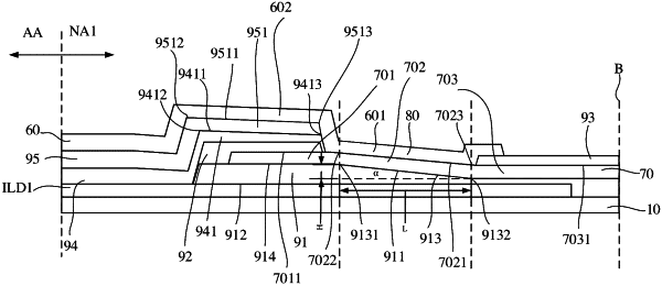
a touch wire electrically connected to at least one touch electrode, wherein at least part of the touch wire extends to the peripheral area;
a touch lead in the peripheral area, wherein the touch lead and the touch wire are located in different conductive layers; and
a contact groove in the peripheral area, wherein the touch wire and the touch lead are in contact with each other in the contact groove,
wherein the touch wire comprises a first touch wire portion in the contact groove, the base substrate has an upper surface close to the pixel units, and the first touch wire portion extends obliquely with respect to the upper surface of the base substrate;
wherein the first touch wire portion is located on a groove bottom of the contact groove;
wherein the touch display panel further comprises a first supporting structure, wherein the first supporting structure comprises a first surface away from the base substrate, the first surface has a first portion, and an orthographic projection of the contact groove on the base substrate substantially coincides with an orthographic projection of the first portion of the first surface on the base substrate,
wherein the first portion of the first surface extends obliquely with respect to the upper surface of the base substrate.
|