| CPC G06F 13/36 (2013.01) [G06F 2213/40 (2013.01)] | 20 Claims |

|
1. A low voltage drive circuit (LVDC) operable to convey data via a bus, the LVDC comprises:
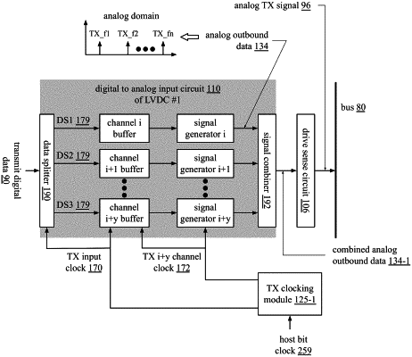
a digital to analog input circuit operable to convert transmit digital data into combined analog outbound data, wherein the transmit digital data has a data rate based on a host input clock, and wherein a first portion of the combined analog outbound data has a first oscillation rate based on a first transmit channel clock and a second portion of the combined analog outbound data has a second oscillation rate based on a second transmit channel clock;
a drive sense circuit operable to:
convert the combined analog outbound data into an analog transmit signal that is transmitted on the bus;
receive an analog receive signal that is transmitted on the bus; and
convert the analog receive signal into analog inbound data; and
a clock circuit operable to:
generate a transmit input clock to synchronize receiving the transmit digital data from a host associated with the host input clock;
generate the first transmit channel clock based on the host input clock; and
generate the second transmit channel clock based on the host input clock.
|