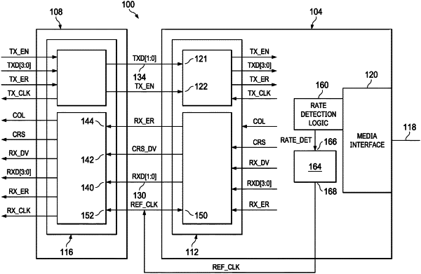
| CPC G06F 13/20 (2013.01) [G06F 1/08 (2013.01)] | 21 Claims |

|
1. An apparatus comprising:
a physical (PHY) layer and a media access control (MAC) layer, the PHY layer including:
a rate detection circuit configured to determine an adopted clock rate for data transmission between the PHY layer and the MAC layer, and in response, provide a rate detection signal indicative of the adopted clock rate;
a reference clock generator having an input coupled to the rate detection circuit and having a reference clock output, the reference clock generator configured to provide at the reference clock output a reference clock signal that is based on the rate detection signal; and
a PHY interface having a data input, a data output, and a clock input, in which the clock input is coupled to the reference clock output; and
the MAC layer including a MAC interface having a clock input coupled to the reference clock output, a data input coupled to the data output of the PHY interface, and a data output coupled to the data input of the PHY interface.
|