| CPC G06F 12/0246 (2013.01) [G06F 7/57 (2013.01); G06F 9/3856 (2023.08); G06F 11/1068 (2013.01); G06F 12/0868 (2013.01); G06F 13/1668 (2013.01); G06F 13/4221 (2013.01)] | 18 Claims |
|
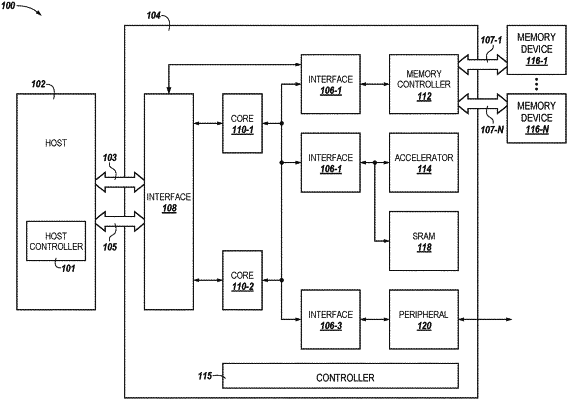
1. An apparatus, comprising:
a plurality of computing devices configured according to a reduced instruction set computing (RISC) architecture;
a first communication subsystem coupled to a host and to each of the plurality of computing devices; and
a plurality of second communication subsystems coupled to each of the plurality of computing devices, wherein each of the plurality of second communication subsystems are coupled to at least one hardware accelerator;
wherein each of the plurality of computing devices are configured to:
perform at least a first portion of an extended memory operation within each respective computing device of the plurality of computing devices without transferring data associated with the first portion of the extended memory operation external to the respective computing device; and
receive a result of performing at least a second portion of the extended memory operation from the at least one hardware accelerator.
|