| CPC G06F 1/08 (2013.01) [G06F 1/10 (2013.01); G06F 1/12 (2013.01)] | 18 Claims |

|
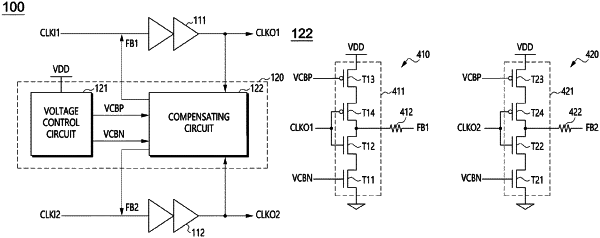
1. A clock generating circuit comprising:
a buffer circuit configured to non-invert an input clock signal to generate an output clock signal;
a voltage control circuit configured to detect a voltage level change of a power voltage and configured to generate a first control voltage and a second control voltage, the first control voltage and the second control voltage having varying voltage levels according to the detected voltage level change; and
a compensating circuit configured to invert the output clock signal according to the first and second control voltages to generate a feedback signal using a single inversion stage, and configured to provide the feedback signal to the input clock signal,
wherein the feedback signal is a single inversion of the output clock signal.
|