| CPC G06F 1/06 (2013.01) [H03B 27/00 (2013.01); H03K 3/0315 (2013.01); H03K 5/133 (2013.01); H03B 2200/0074 (2013.01)] | 12 Claims |
|
1. A circuit for a multi-phase clock generator, comprising:
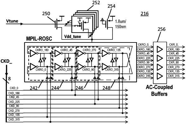
a delay line comprising a first plurality of differential unit delay cells,
wherein each of the first plurality of differential unit delay cells has a pair of clock inputs and a pair clock outputs,
wherein the first plurality of differential unit delay cells are connected in series such that the pair of clock outputs of a first of the first plurality of differential unit delay cells is connected to the pair of clock inputs of a second of the first plurality of differential unit delay cells, and
wherein each unit cell of the first plurality of differential unit delay cells outputs a pair of clock signals having different phases than each pair of clock signals output by other of the first plurality of differential unit delay cells; and
a ring oscillator comprising a second plurality of differential unit delay cells,
wherein each of the second plurality of differential unit delay cells has a pair of clock inputs, a pair of current injection inputs, and a pair clock outputs,
wherein the pair of current injection inputs of each of the second plurality of differential unit delay cells is coupled to the pair of clock outputs of a corresponding one of the first plurality of differential unit delay cells,
wherein the second plurality of differential unit delay cells are connected in series such that the pair of clock outputs of a first of the second plurality of differential unit delay cells is connected to the pair of inputs of a second of the second plurality of differential unit delay cells,
wherein the pair of outputs of a last of the second plurality of differential unit delay cells are flipped and connected to the pair of inputs of a first of the second plurality of differential unit delay cells, and
wherein each unit cell of the second plurality of differential unit cells outputs a pair of clock signals having different phases than each pair of clock signals output by other of the second plurality of differential unit delay cells,
wherein the delay line further comprises a dummy unit cell connected to a last of the first plurality of differential unit delay cells.
|