| CPC G03F 7/162 (2013.01) [B05B 13/0228 (2013.01); B05B 15/50 (2018.02); B05B 15/55 (2018.02); B05C 11/02 (2013.01); B05D 1/02 (2013.01); H01L 21/67017 (2013.01); H01L 21/67051 (2013.01); H01L 21/6708 (2013.01); H01L 21/6715 (2013.01); B05B 1/24 (2013.01)] | 5 Claims |

|
1. A semiconductor fabrication method, comprising:
coating a photoresist on a substrate;
heating the substrate to cure the photoresist;
exposing the photoresist to light; and
developing the photoresist to form a photoresist pattern, wherein coating the photoresist includes:
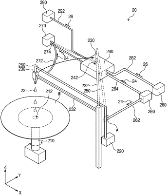
providing the photoresist on the substrate by supplying the photoresist to a nozzle connected to a photoresist pipeline;
driving the nozzle to move toward a nozzle housing;
supplying a solvent into a solvent storage groove of a lower housing of the nozzle housing;
supplying a purge gas into a nozzle insert hole of an upper housing on the lower housing;
inhaling a first portion of the purge gas into a tip of the nozzle; and
inhaling a portion of the solvent into the tip of the nozzle,
wherein the photoresist pipeline includes:
an external line;
an internal line in the external line; and
a filler between an inner wall of the external line and an outer wall of the internal line, the filler containing the purge gas.
|