US 12,189,266 B2
Active photonic devices incorporating high dielectric constant materials
Chia-Ming Chang, Palo Alto, CA (US); Hung-Hsi Lin, San Jose, CA (US); and Gary Gibson, Palo Alto, CA (US)
Assigned to Psiquantum, Corp., Palo Alto, CA (US)
Filed by Psiquantum, Corp., Palo Alto, CA (US)
Filed on Oct. 27, 2023, as Appl. No. 18/384,802.
Application 18/384,802 is a continuation of application No. 18/112,415, filed on Feb. 21, 2023, granted, now 11,841,559.
Application 18/112,415 is a continuation of application No. 17/326,233, filed on May 20, 2021, granted, now 11,624,964, issued on Apr. 11, 2023.
Application 17/326,233 is a continuation of application No. 16/697,704, filed on Nov. 27, 2019, granted, now 11,036,111, issued on Jun. 15, 2021.
Application 16/697,704 is a continuation of application No. 16/365,543, filed on Mar. 26, 2019, granted, now 10,627,696, issued on Apr. 21, 2020.
Claims priority of provisional application 62/819,765, filed on Mar. 18, 2019.
Prior Publication US 2024/0134243 A1, Apr. 25, 2024
Prior Publication US 2024/0231175 A9, Jul. 11, 2024
Int. Cl. G02F 1/225 (2006.01); G02F 1/21 (2006.01)
CPC G02F 1/2257 (2013.01) [G02F 1/212 (2021.01); G02F 2203/50 (2013.01)] 20 Claims
OG exemplary drawing
 
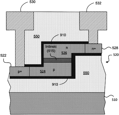
1. A waveguide structure comprising:
a substrate;
a waveguide core coupled to the substrate and including a first material characterized by a first index of refraction and a first electro-optic coefficient;
a first cladding layer at least partially surrounding the waveguide core and including a second material characterized by a second index of refraction less than the first index of refraction and a second electro-optic coefficient greater than the first electro-optic coefficient; and
a second cladding layer coupled to the first cladding layer, wherein the first cladding layer is disposed between the waveguide core and the second cladding layer.