| CPC G02F 1/2255 (2013.01) [G02F 1/0121 (2013.01); G02F 1/035 (2013.01); G02F 1/0356 (2013.01); G02F 1/212 (2021.01); H05K 1/02 (2013.01)] | 9 Claims |

|
1. An optical modulator comprising:
an optical modulation element that includes a plurality of signal electrodes;
a plurality of signal input terminals each of which inputs an electrical signal to be applied to each of the plurality of signal electrodes;
a relay substrate having, on a surface of the relay substrate, a plurality of signal conductor patterns that electrically connect the plurality of signal input terminals to the plurality of signal electrodes, and a plurality of ground conductor patterns; and
a housing that accommodates the optical modulation element and the relay substrate,
wherein among sides of the relay substrate, a signal input side on which the plurality of signal input terminals is connected to the plurality of signal conductor patterns and a signal output side on which the plurality of signal conductor patterns is connected to the plurality of signal electrodes face each other in a plan view, and
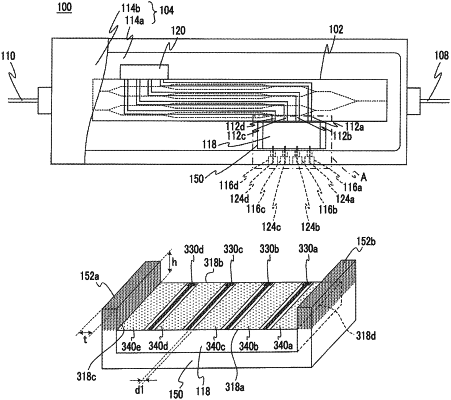
an electromagnetic wave propagation suppressing unit made of a material that absorbs electromagnetic waves and protruding to a height higher than any of the plurality of signal conductor patterns and the plurality of ground conductor patterns of the relay substrate is provided along at least one side connecting an end portion of the signal input side and an end portion of the signal output side in the plan view, among the sides of the relay substrate.
|