| CPC G02F 1/225 (2013.01) [G02F 1/212 (2021.01); G02F 2203/10 (2013.01); H01L 21/768 (2013.01)] | 14 Claims |
|
1. An optoelectronic device, comprising:
a semiconductor substrate;
thin film structures disposed on the substrate and patterned to define components of an integrated drive circuit, which is configured to generate a drive signal;
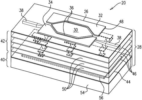
a back end of line (BEOL) stack of alternating metal layers and dielectric layers disposed over the thin film structures, the metal layers comprising:
a modulator layer, which is a final, outer layer of the BEOL stack and comprises gold, and which contains a plasmonic waveguide and is patterned to define a plurality of electrodes, which are configured to apply a modulation to surface plasmons polaritons (SPPs) propagating in the plasmonic waveguide in response to the drive signal applied to the electrodes; and
a plurality of interconnect layers, which are patterned to define electrical traces, which are connected by vias to the thin film structures on the substrate and to the electrodes in the modulator layer so as to interconnect the components of the integrated drive circuit and to apply the drive signal generated thereby to the electrodes;
an optical input coupler, which is configured to couple light into the modulator layer, whereby the light is modulated by the modulation of the SPPs; and
an optical output coupler, which is configured to couple the modulated light out of the modulator layer.
|