| CPC G02F 1/136286 (2013.01) [G02F 1/133388 (2021.01); G02F 1/1345 (2013.01); G02F 1/136218 (2021.01); G02F 1/136222 (2021.01); G02F 1/1368 (2013.01); G02F 2201/121 (2013.01); G09G 3/3655 (2013.01); G09G 2300/0413 (2013.01)] | 16 Claims |

|
1. A display panel, comprising a display region and a redundancy pixel region located on at least one side of the display region, wherein the display panel comprises:
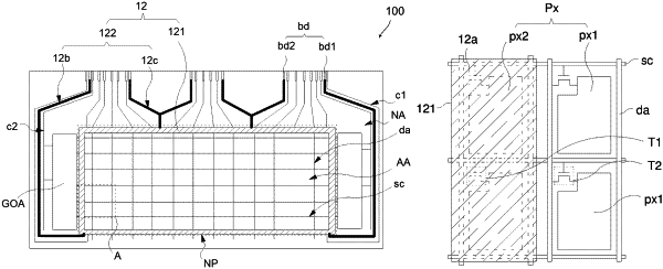
an array substrate comprising a first base and a common wiring disposed on the first base, wherein the common wiring comprises a first wiring, and the first wiring is disposed in the redundancy pixel region;
an opposite substrate disposed opposite to the array substrate, wherein the opposite substrate comprises a second base and a common electrode layer disposed on a side of the second base near the array substrate, and the common electrode layer is disposed in the display region and the redundancy pixel region; and
a liquid crystal layer, the liquid crystal layer disposed between the array substrate and the opposite substrate and extending in the redundancy pixel region and the display region, wherein the liquid crystal layer in the redundancy pixel region is located between the first wiring and the common electrode layer;
wherein, along a thickness direction of the display panel, the first wiring overlaps the common electrode layer, when the display panel is in a display state, under a LO grayscale of a viewing angle of 0 degree, image brightness of an overlapping region between the first wiring and the common electrode layer ranges from 0 to 0.0017 lux;
wherein the array substrate further comprises a thin film transistor array layer, an insulation layer, and a pixel electrode layer, the thin film transistor array layer is disposed on the first base, the insulation layer is disposed on the thin film transistor array layer, and the pixel electrode layer is disposed on the insulation layer;
wherein the pixel electrode layer comprises a pixel electrode and a redundancy pixel electrode, the pixel electrode is disposed in the display region, the redundancy pixel electrode is disposed in the redundancy pixel region, and at least one part of the redundancy pixel electrode is multiplexed as a part of the first wiring;
wherein the first wiring further comprises a connection portion, and in the redundancy pixel region, the connection portion is connected between the first wiring and the redundancy pixel electrode to form an entire plate structure or a patterned structure.
|