| CPC G02F 1/13338 (2013.01) [G02F 1/133345 (2013.01); G02F 1/133514 (2013.01); G02F 1/134309 (2013.01); G02F 1/13439 (2013.01); G02F 1/136286 (2013.01); G02F 1/1368 (2013.01); G06F 3/041 (2013.01); G06F 3/0412 (2013.01); G06F 3/0443 (2019.05); G06F 3/047 (2013.01); G02F 1/133302 (2021.01); G02F 1/134372 (2021.01); G02F 1/136295 (2021.01); G06F 2203/04103 (2013.01)] | 19 Claims |

|
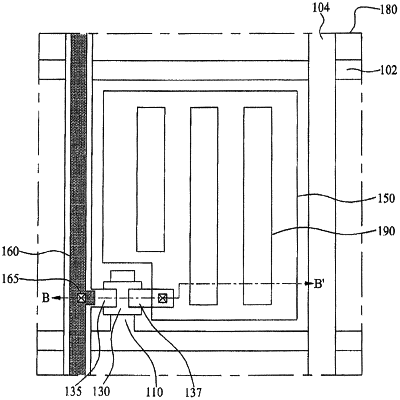
1. A display device, comprising:
a first data line electrically connected to a first thin film transistor;
a first pixel electrode electrically connected with the first thin film transistor via a first pixel electrode contact hole;
a second data line electrically connected to a second thin film transistor;
a second pixel electrode electrically connected with the second thin film transistor via a second pixel electrode contact hole;
a first touch sensing electrode corresponding to the first pixel electrode and insulated from the first pixel electrode;
a second touch sensing electrode corresponding to the second pixel electrode and insulated from the second pixel electrode;
a first sensing line electrically connected with the first touch sensing electrode; and
a second sensing line electrically connected with the second touch sensing electrode,
wherein the first data line overlaps with the first touch sensing electrode and the second touch sensing electrode,
wherein the second data line overlaps with the first touch sensing electrode and the second touch sensing electrode,
wherein the first sensing line overlaps with the first touch sensing electrode and the second touch sensing electrode, and does not overlap with the second sensing line within areas of the display device overlapping with the first touch sensing electrode or the second touch sensing electrode in a plan view, and
wherein the second sensing line overlaps with the second touch sensing electrode.
|
|
15. A display device, comprising:
a first data line electrically connected to a first thin film transistor;
a first pixel electrode electrically connected with the first thin film transistor via a first pixel electrode contact hole;
a second data line electrically connected to a second thin film transistor;
a second pixel electrode electrically connected with the second thin film transistor via a second pixel electrode contact hole;
a first touch sensing electrode corresponding to the first pixel electrode and insulated from the first pixel electrode;
a second touch sensing electrode corresponding to the second pixel electrode and insulated from the second pixel electrode;
a first sensing line electrically connected with the first touch sensing electrode; and
a second sensing line electrically connected with the second touch sensing electrode,
wherein the first data line overlaps with the first touch sensing electrode and the second touch sensing electrode,
wherein the second data line overlaps with the first touch sensing electrode and the second touch sensing electrode, and
wherein:
the first data line is formed in a curved-line shape and is parallel with the first sensing line, and the second data line is formed in a curved-line shape and is parallel with the second sensing line.
|