| CPC G02F 1/13318 (2013.01) [G02F 1/134336 (2013.01); H10K 50/813 (2023.02); H10K 50/822 (2023.02); H10K 59/352 (2023.02); H10K 59/353 (2023.02); G02F 1/134318 (2021.01); G02F 1/1368 (2013.01); G02F 2201/52 (2013.01); G09G 2300/0452 (2013.01); H10K 59/12 (2023.02)] | 19 Claims |

|
1. A display device, comprising:
a substrate including a first pixel, and a second pixel, the second pixel neighboring the first pixel;
a plurality of scan lines, a first driving gate electrode, and a second driving gate electrode disposed on the substrate, the scan lines extending in a first direction;
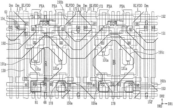
a first semiconductor pattern extending with a first width, a portion of the first semiconductor pattern overlapping the first driving gate electrode in the first pixel forms a first channel portion with the first width,
a second semiconductor pattern extending with a second width, a portion of the second semiconductor pattern overlapping the second driving gate electrode in the second pixel forms a second channel portion with the second width; and
a plurality of data lines and a plurality of driving voltage lines disposed on the substrate and crossing the scan lines and extending in a second direction perpendicular to the first direction, wherein
the first channel portion with the first width has two opposing edges extending parallel to each other and curved at least two times,
the first channel portion includes a first portion extending in the second direction and having a first end, a second portion extending in the first direction and having a second end connected to the first end, and a third end opposing the second end, and a third portion extending in the second direction and having a fourth end connected to the third end and a fifth end opposing the fourth end,
the first portion and the third portion are disposed at a same side with respect to the second portion,
a shape of the first channel portion is different from a shape of the second channel portion, and
a length of the first channel portion is different from a length of the second channel portion, wherein
the shape of the first channel portion is defined by outer edges of the first semiconductor pattern, and
the shape of the second channel portion is defined by outer edges of the second semiconductor pattern.
|