| CPC G02B 6/4255 (2013.01) [G02B 6/4239 (2013.01); G02B 6/4293 (2013.01); G02B 6/43 (2013.01)] | 20 Claims |

|
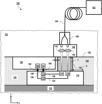
1. A method for manufacturing an integrated circuit (IC) package, comprising:
providing a base assembly comprising a photonic integrated circuit (PIC), the PIC comprising an active element, a coupling element at a surface of the PIC, and one or more waveguides providing an optical path through the PIC between the optical coupling element and the active element for light in an operative wavelength band of the PIC;
attaching a first spacer to a surface of the base assembly over a first portion of the PIC including the optical coupling element, the spacer being transparent for light in the operative wavelength band;
attaching a first electrical IC (EIC) to the surface of the base assembly overlapping a second portion of the PIC away from the optical coupling element;
depositing a first molding compound over the first spacer and the first EIC to form a layer of the first molding compound encapsulating the first EIC and the first spacer; and
removing a first portion of the first molding compound from the layer of the first molding compound to expose a surface of the first spacer opposite the PIC.
|