| CPC G02B 6/4214 (2013.01) [G02B 6/428 (2013.01); H01L 25/167 (2013.01)] | 20 Claims |

|
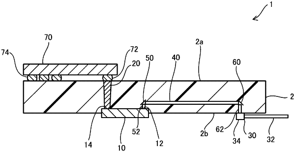
1. A semiconductor package, comprising:
a printed wiring board;
a logic IC mounted on a first surface of the printed wiring board;
a connector mounted on a second surface of the printed wiring board on an opposite side of the printed wiring board with respect to the first surface;
an optical element configured to convert an optical signal and an electrical signal and positioned on the opposite side of the printed wiring board with respect to the first surface such that the optical element is at least partially embedded in the printed wiring board;
a path formed in the printed wiring board and configured to electrically connect the logic IC on the first surface of the printed wiring board and the optical element on the opposite side of the printed wiring board with respect to the first surface; and
an optical waveguide embedded on the opposite side of the printed wiring board with respect to the first surface and configured to optically connect the connector on the second surface of the printed wiring board and the optical element on the opposite side of the printed wiring board with respect to the first surface,
wherein the path is formed substantially straight and substantially perpendicular to the first surface of the printed wiring board, and the logic IC and the optical element are positioned such that the logic IC and the optical element at least partially overlap.
|