| CPC G02B 1/11 (2013.01) [G02B 3/04 (2013.01); G02B 7/021 (2013.01); G02B 27/0018 (2013.01)] | 14 Claims |

|
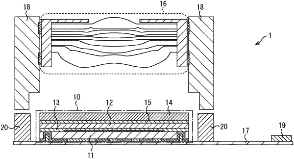
1. An imaging device, comprising:
a solid-state imaging element including a laminate substrate, wherein
the laminate substrate includes a first substrate and a second substrate,
and
the first substrate and the second substrate are laminated;
a glass substrate above the first substrate, wherein
the glass substrate includes a first glass substrate and a second glass substrate, and
the first glass substrate is bonded to the second glass substrate;
a lens on the glass substrate; and
a cavity between the lens and the solid-state imaging element.
|