| CPC G01R 31/318597 (2013.01) | 8 Claims |

|
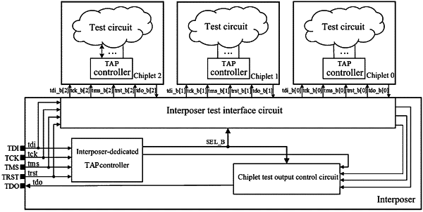
1. A circuit for post-binding testing of a 2.5D chiplet, wherein a parallel testing is performed on a multi-chiplet integrated circuit comprising N chiplets, the circuit for post-binding testing of the 2.5D chiplet comprising:
an interposer-dedicated TAP controller configured to receive a configuration vector from a port of a chip JTAG and output a control signal for determining tested chiplets under parallel testing and an output sequence of test output signals;
an interposer test interface circuit configured to receive a test vector from the port of the chip JTAG, and when receiving the control signal output by the interposer-dedicated TAP controller, to connect to a test data input port, a test clock signal input port, a test mode selection signal input port, a test reset signal input port and a test data output port of the tested chiplets under parallel testing, where a test clock signal of each tested chiplet that is generated according to the control signal output by the interposer-dedicated TAP controller and a test clock input signal from the port of the chip JTAG is transmitted to the test clock signal input port of each tested chiplet, a test mode selection signal of each tested chiplet that is generated according to the control signal output by the interposer-dedicated TAP controller and a test mode selection signal from the port of the chip JTAG is transmitted to the test mode selection signal input port of each tested chiplet, a test data input signal of each tested chiplet that is shifted in according to the test clock signal of each tested chiplet is transmitted to the test data input port of each tested chiplet, a test reset signal from the port of the chip JTAG is transmitted to the test reset signal input port of each tested chiplet, and a test output signal of each tested chiplet is transmitted to a chiplet test output control circuit; and
the chiplet test output control circuit configured to receive the control signal output by the interposer-dedicated TAP controller, and sequentially transmit the test output signal of each tested chiplet to the port of the chip JTAG.
|