| CPC G01N 27/4145 (2013.01) [G01N 27/4146 (2013.01)] | 16 Claims |

|
1. A method for forming a nanopore transistor for biosensing, the method comprising:
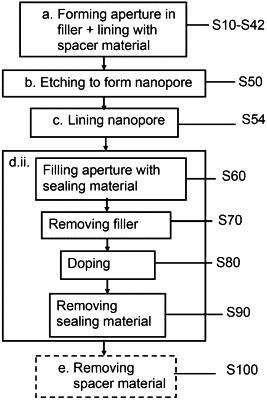
(a) forming an aperture in a filler material by:
(i) providing a fin structure comprising at least a bottom semiconductor layer and a top layer;
(ii) patterning the top layer to form a pillar;
(iii) laterally embedding the pillar in the filler material;
(iv) forming the aperture in the filler material by removing the pillar;
(v) lining the aperture with a spacer material, thereby reducing a size of the aperture;
(b) forming a nanopore in the bottom semiconductor layer by etching through the aperture;
(c) lining the nanopore with a gate dielectric material, thereby forming a gate dielectric; and
(d) forming a source and a drain by either:
(i) between steps a.ii and a.iii, doping the bottom semiconductor layer by ion implantation using the pillar as a mask, or
(ii) after step b,
filling the aperture with a sealing material so that the sealing material is coplanar with the filler material, thereby forming a post comprising the sealing material and the spacer material;
removing the filler material selectively with respect to the post, thereby exposing a part of the bottom semiconductor layer;
doping the bottom semiconductor layer by ion implantation by using the post as a mask; and
removing the sealing material.
|