| CPC G01N 27/327 (2013.01) [A61B 5/24 (2021.01); C09D 11/52 (2013.01); G01N 27/30 (2013.01); H05K 3/0085 (2013.01); H05K 3/125 (2013.01); B33Y 10/00 (2014.12); B33Y 70/10 (2020.01); B33Y 80/00 (2014.12)] | 17 Claims |

|
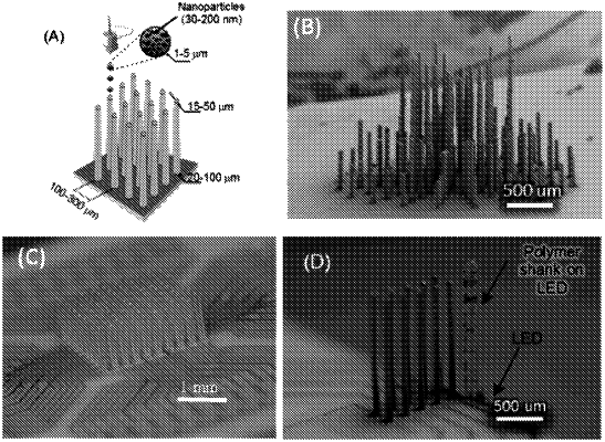
1. A method of preparing a high-density array of electrically-conductive, or optically-conductive shanks, comprising:
depositing by aerosol jet printing, a plurality of shanks onto a surface of a substrate in a density of greater than 100 shanks per square centimeter of the surface of the substrate, each shank having a diameter ranging from 10 μm to 1 mm, and a length ranging from 10 μm to 10 cm, wherein the shanks are formed by depositing over the surface of the substrate a plurality of layers of a shank material solution comprising a conductive material dispersed in a liquid or a waveguide-forming material in a solvent, where each layer of the plurality of layers is deposited as an open shape having ends and a gap defined by the ends.
|