| CPC G01B 11/2441 (2013.01) [G01B 11/30 (2013.01); G01B 2210/56 (2013.01)] | 2 Claims |

|
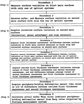
1. A method for measuring a wafer profile while holding a periphery of the wafer by using a flatness measurement system in which the wafer is placed, and which includes a first optical system and a second optical system respectively located on a first main surface and a second main surface of the wafer, the method comprising:
a first step of measuring each of a surface variation on the first main surface and a surface variation on the second main surface of the wafer by using only one optical system of the first optical system and the second optical system, wherein
the wafer is placed into the flatness measurement system to measure the surface variation on the first main surface with only the one optical system, and
the surface variation on the second main surface is measured with only the one optical system such that the wafer is placed into the flatness measurement system while being reversed with respect to a state of the wafer placed to measure the surface variation on the first main surface;
a second step of calculating a periphery-holding deformation amount, which is caused by holding the periphery of the wafer, through utilization of the surface variation on the first main surface and the surface variation on the second main surface measured with the one optical system, the second step comprising:
acquiring a first thickness unevenness of the wafer, wherein
the surface variation on the second main surface measured in the first step is corrected to acquire a corrected surface variation on the second main surface, and
the first thickness unevenness is acquired from a difference between the surface variation on the first main surface measured in the first step and the corrected surface variation on the second main surface;
acquiring a second thickness unevenness of the wafer from a difference between the surface variation on the first main surface measured with the one optical system and a surface variation on the second main surface measured with the other optical system; and
acquiring the periphery-holding deformation amount, wherein
an average value of the first thickness unevenness and an average value of the second thickness unevenness are calculated,
a difference between the average value of the second thickness unevenness and the average value of the first thickness unevenness is added to the first thickness unevenness to acquire a revised first thickness unevenness, and
a value that is ½ of a difference between the revised first thickness unevenness and the second thickness unevenness is set to the periphery-holding deformation amount; and
a third step of calculating an actual Warp value of the wafer through subtraction of the periphery-holding deformation amount from a Warp value outputted by the flatness measurement system.
|