| CPC C30B 29/36 (2013.01) [C30B 25/20 (2013.01); H01L 21/6836 (2013.01); H01L 21/78 (2013.01); H01L 21/7813 (2013.01); H01L 29/1608 (2013.01); H01L 2221/68327 (2013.01)] | 4 Claims |
|
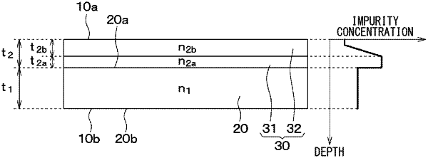
1. A silicon carbide wafer comprising:
a base wafer made of silicon carbide, having a first main surface and a second main surface opposite to the first main surface, and doped with an n-type impurity; and
an epitaxial layer arranged on the first main surface of the base wafer, made of silicon carbide and doped with an n-type impurity, wherein
a thickness of the base wafer is referred to as t1, a thickness of the epitaxial layer is referred to as t2, a ratio of the thickness of the epitaxial layer to the thickness of the base wafer is referred to as a thickness ratio t2/t1, an average impurity concentration of the base wafer is referred to as n1, an average impurity concentration of the epitaxial layer is referred to as n2, and a ratio of the average impurity concentration of the epitaxial layer to the average impurity concentration of the base wafer is referred to as an average impurity concentration ratio n2/n1, and the base wafer and the epitaxial layer are configured so that the thickness ratio t2/t1 and the average impurity concentration ratio n2/n1 satisfy a mathematical formula 1:
−0.0178<0.012+(t2/t1)×0.057−(n2/n1)×0.029−{(t2/t1)−0.273}×{(n2/n1)−0.685}×0.108<0.0178. [Formula 1]
|