| CPC C30B 25/16 (2013.01) [C23C 16/46 (2013.01); C23C 16/52 (2013.01); C30B 25/10 (2013.01); H01L 21/0254 (2013.01); H01L 21/0262 (2013.01); H01L 22/20 (2013.01)] | 10 Claims |

|
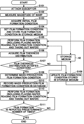
1. A method of manufacturing a semiconductor device, comprising:
attaching a first susceptor to a film forming apparatus;
measuring a magnitude of a warp of the first susceptor;
setting a first initial film formation condition as a film formation condition of the film forming apparatus in accordance with the measured magnitude of the warp of the first susceptor; and
placing a plurality of first wafers on the first susceptor and forming a first film on the plurality of first wafers under the film formation condition,
wherein the setting of the first initial film formation condition includes reading the first initial film formation condition from a recording medium storing a database, and
wherein the database includes a plurality of pieces of data in which magnitudes of warps of susceptors are associated with initial film formation conditions for forming the first film.
|