| CPC B81C 1/00293 (2013.01) [B81B 7/0041 (2013.01); B81B 2201/0271 (2013.01); B81B 2201/032 (2013.01); B81C 2203/0145 (2013.01)] | 20 Claims |

|
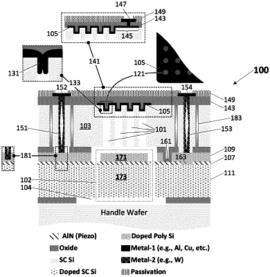
1. An integrated circuit comprising:
a layer stack, including a first silicon layer, a second silicon layer, and an oxide layer between the first silicon layer and the second silicon layer;
a chamber within the layer stack, between the first silicon layer and the second silicon layer;
a microelectromechanical systems (MEMS) component within the layer stack, the MEMS component having a piezoelectric layer;
an electrode within the layer stack, and a conductive path that connects the electrode with an electrical contact on an exterior surface of the integrated circuit, the conductive path being configured so as to provide an output signal, from the electrode, representing sensed motion of the MEMS component;
a passageway extending through the one of the first silicon layer and the second silicon layer, the passageway having at least one bend so as to prevent line-of-sight view through the one of the first silicon layer and the second silicon layer;
the chamber being formed at least in part by removal of oxide from the oxide layer, via the passageway, such that the MEMS component is free to deflect or move within the chamber; and
at least one material deposited so as to block the passageway, following the removal of the oxide, in a region in between the at least one bend and an exterior surface of the integrated circuit, wherein the at least one bend is configured so as to inhibit deposition ingress of the at least one material into the chamber.
|