| CPC B81B 7/0061 (2013.01) [B81B 2201/0257 (2013.01); B81B 2207/012 (2013.01); H01L 2224/48137 (2013.01); H01L 2224/73265 (2013.01); H01L 2924/15151 (2013.01)] | 20 Claims |
|
1. A semiconductor device, comprising:
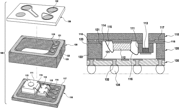
a cavity substrate comprising a substrate top side, a substrate bottom side, a substrate sidewall joining the substrate top side to the substrate bottom side, and a cavity through the substrate top side, wherein the cavity comprises a cavity bottom surface and a cavity sidewall, wherein an inner surface of the cavity sidewall extends from the cavity bottom surface to the substrate top side, and wherein the inner surface of the cavity sidewall and an outer surface of the substrate sidewall define a wall thickness of the substrate sidewall;
an electrical component in the cavity of the cavity substrate;
a planar substrate coupled to the substrate top side, wherein the planar substrate covers the electrical component in the cavity of the cavity substrate;
conductive lands on an external surface of the semiconductor device; and
one or more conductive paths traversing the cavity sidewall and coupling the conductive lands to the electrical component; and
wherein a conductive path of the one or more conductive paths comprises:
a first surface in direct contact with the inner surface of the cavity sidewall; and
a second surface, opposite the first surface, that is exposed.
|