| CPC B32B 27/08 (2013.01) [H01L 23/373 (2013.01); H05K 1/0373 (2013.01)] | 24 Claims |
|
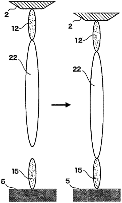
1. A laminate, comprising:
a thermally conductive first inorganic filler bonded with one end of a first coupling agent;
a thermally conductive second inorganic filler bonded with one end of a second coupling agent, in which a bifunctional or higher functional polymerizable liquid crystal compound is further bonded with the other end of the second coupling agent, a filler bonded with at least one functional group of the polymerizable liquid crystal compound in the other end of the first coupling agent; and
a metal layer bonded with one end of a third coupling agent,
wherein the other end of the third coupling agent is bonded with the other end of the first coupling agent.
|