| CPC B29C 43/24 (2013.01) [B29C 43/021 (2013.01); B29C 59/005 (2013.01); B29C 59/026 (2013.01); B29K 2995/0005 (2013.01); B29K 2995/0007 (2013.01); B29L 2031/3406 (2013.01); H10K 71/821 (2023.02); H10K 77/10 (2023.02)] | 6 Claims |

|
1. A method for manufacturing a substrate of an optoelectronic component comprising a stack of layers, the method comprising a step of:
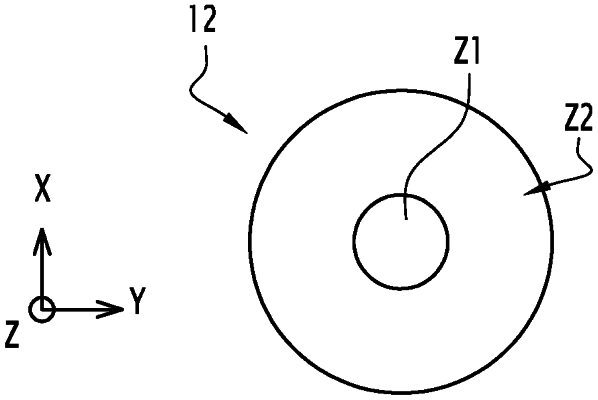
preforming a substrate comprising a face having a pattern with at least one zone made of a first material and a zone made of a second material, wherein the first material and the second material each are thermosetting or thermoplastic materials, wherein the first material is an electrically conductive material and the second material is an electrically insulating material, wherein the face of the substrate is planar, and wherein the zone made of the second material completely surrounds the at least one zone made of the first material,
and
molding by compression the face of the substrate with a face of a reference element presenting a surface roughness less than or equal to 50 nanometers.
|