| CPC H02J 7/00 (2013.01) [H01L 23/49503 (2013.01); H01L 23/49562 (2013.01); H01L 23/49575 (2013.01); H01L 23/528 (2013.01); H01L 23/62 (2013.01); H01L 25/072 (2013.01); H01L 27/0248 (2013.01); H01L 27/088 (2013.01); H01L 27/0883 (2013.01); H01L 29/1033 (2013.01); H01L 29/2003 (2013.01); H01L 29/402 (2013.01); H01L 29/41758 (2013.01); H02M 1/088 (2013.01); H02M 3/157 (2013.01); H02M 3/1584 (2013.01); H02M 3/1588 (2013.01); H03K 3/012 (2013.01); H03K 3/356017 (2013.01); H03K 17/102 (2013.01); H03K 19/018507 (2013.01); H01L 2924/00 (2013.01); H01L 2924/0002 (2013.01); H02M 1/0048 (2021.05); H02M 3/155 (2013.01); Y02B 40/00 (2013.01); Y02B 70/10 (2013.01)] | 8 Claims |
|
6. An electronic component comprising:
a package base;
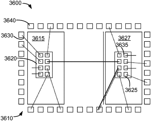
one or more semiconductor dies secured to the package base and comprising:
a first transistor having a first gate terminal, a first source terminal and a first drain terminal; and
a second transistor having a second gate terminal, a second source terminal and a second drain terminal;
wherein the first drain terminal is coupled to the second source terminal;
wherein the first transistor is a gallium nitride (GaN)-based lateral high electron mobility transistor (HEMT) and the second transistor is a GaN-based lateral HEMT;
wherein the one or more semiconductor dies comprise a first and second GaN-based dies and a third silicon-based die, and wherein the first transistor is disposed on the first GaN-based die, the second transistor is disposed on the second GaN-based die, and wherein the third silicon-based die comprises a first gate driver circuit coupled to the first gate terminal.
|