| CPC H10N 70/823 (2023.02) [H10B 63/80 (2023.02); H10N 70/063 (2023.02); H10N 70/841 (2023.02); H10N 70/24 (2023.02); H10N 70/883 (2023.02); H10N 70/8833 (2023.02)] | 20 Claims |
|
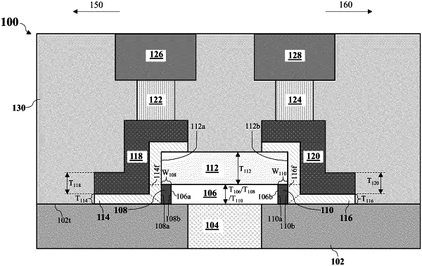
1. A memory device comprising:
a first electrode comprising a first side surface and a second side surface opposite to the first side surface;
a passivation layer arranged laterally alongside the first side surface of the first electrode;
a switching layer arranged laterally alongside the passivation layer;
a second electrode arranged along the switching layer; and
an insulating element arranged over the first electrode and the passivation layer; wherein the switching layer is arranged over the insulating element.
|