|
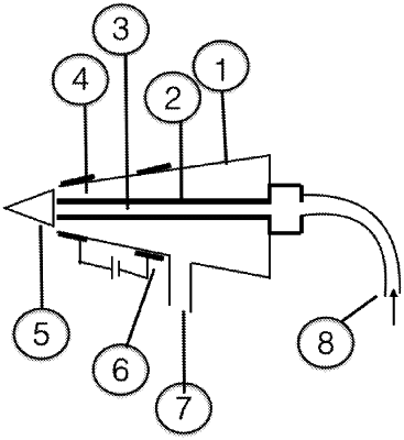
1. A plasma jet printer for high throughput direct write printing of conducting electronic materials comprising: two non-concentric tubes, with an inner tube located inside an outer tube; said inner tube having at a first end an inlet through which an aerosol of electronic materials is introduced, said outer tube having a gas inlet through which a gas is introduced, an electrode assembly on the outer tube connected to a high voltage power supply for creating a plasma from said gas between the inner tube and the outer tube; a nebulizer connected to the inlet at the first end of the inner tube for generating the aerosol of electronic materials; said inner tube having a second end through which said aerosol of electronic materials exits; said outer tube having discharge end through which said plasma is discharged; said second end of said inner tube and said discharge end of said outer tube located in a common plane; and a substrate placed adjacent said second end of said inner tube and said discharge end of said outer tube to receive said discharged plasma and aerosol of electronic materials.
|