| CPC H10B 63/84 (2023.02) [G11C 5/12 (2013.01); G11C 13/0002 (2013.01); H01L 21/823487 (2013.01); H01L 27/1225 (2013.01); H01L 29/4908 (2013.01); H01L 29/66666 (2013.01); H01L 29/66795 (2013.01); H01L 29/7827 (2013.01); H01L 29/7869 (2013.01); H01L 29/78642 (2013.01); H01L 29/78696 (2013.01); H10B 63/22 (2023.02); H10B 63/24 (2023.02); H10B 63/34 (2023.02); H10N 70/011 (2023.02); H10N 70/245 (2023.02); H10N 70/828 (2023.02); H10N 70/841 (2023.02); H10N 70/883 (2023.02); G11C 11/1659 (2013.01); G11C 11/2259 (2013.01); G11C 11/401 (2013.01); G11C 13/003 (2013.01); G11C 2213/79 (2013.01); H01L 29/78618 (2013.01)] | 18 Claims |
|
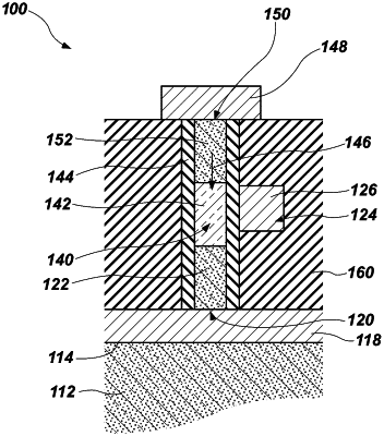
1. A method of forming a semiconductor device, the method comprising:
forming a hybrid transistor supported by a substrate comprising:
forming a source including a first low bandgap high mobility material;
forming a channel including a high bandgap low mobility material coupled with the first low bandgap high mobility material;
forming a drain including a second low bandgap high mobility material coupled with the high bandgap low mobility material; and
forming a gate separated from the channel via a gate oxide material,
wherein forming the channel includes forming the high bandgap low mobility material to have a length that is shorter than a length of the gate.
|