| CPC H10B 43/27 (2023.02) [H01L 21/02532 (2013.01); H01L 21/02636 (2013.01); H01L 21/31111 (2013.01); H01L 21/31144 (2013.01); H01L 29/40117 (2019.08); H10B 43/35 (2023.02)] | 10 Claims |
|
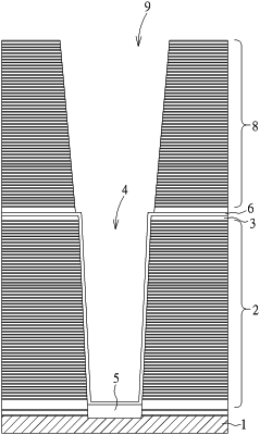
1. A method of forming a structure of 3D NAND memory device, comprising:
forming a first stack layer on a substrate;
forming a first channel hole extending through said first stack layer;
forming a block layer on a surface of said first stack layer and on a sidewall of said first channel hole;
forming a sacrificial layer in said first channel hole;
forming a second stack layer on said first stack layer and said sacrificial layer;
performing a first etch process to form a second channel hole extending through said second stack layer and completely overlapping said first channel hole and to remove said sacrificial layer in said first channel hole, wherein a minimum diameter of said second channel hole is larger than a maximum diameter of said first channel hole;
removing said block layer exposed from said second channel hole; and
forming a function layer on a surface of said first channel hole and said second channel hole.
|