| CPC H10B 43/20 (2023.02) [H01L 29/66795 (2013.01); H01L 29/7851 (2013.01); H10B 41/20 (2023.02)] | 12 Claims |
|
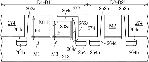
1. A method of forming a silicon-oxide-nitride-oxide-silicon (SONOS) memory cell for FinFET, comprising:
forming a fin on a top surface of a substrate, wherein the fin comprises a memory region and a logic region;
sequentially depositing a charge trapping material and a control gate material covering the fin and the substrate blanketly;
patterning the control gate material and the charge trapping material to form a charge trapping layer and a control electrode over the fin of the memory region;
sequentially depositing a dielectric layer and a gate electrode layer covering the fin and the substrate blanketly;
patterning the gate electrode layer and the dielectric layer to form a gate in the logic region and a selective gate in the memory region adjacent to the control gate; and
replacing the selective gate and the gate by a selective metal gate and a metal gate respectively.
|