| CPC H10B 41/27 (2023.02) [G11C 5/06 (2013.01); H01L 29/66666 (2013.01); H01L 29/7827 (2013.01); H10B 43/27 (2023.02)] | 24 Claims |
|
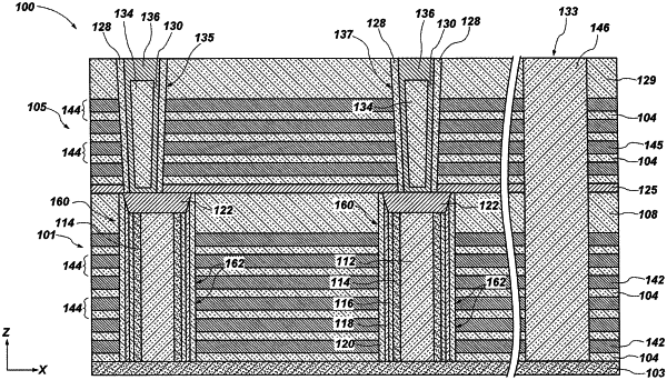
1. A microelectronic device, comprising:
a stack structure comprising a vertically alternating sequence of conductive structures and insulative structures arranged in tiers, the stack structure divided into block structures separated from one another by slot structures;
lower pillars vertically extending through the block structures of the stack structure, the lower pillars exhibiting pillar bending in a first direction, each of the lower pillars having a lowermost surface and an uppermost surface that is not vertically aligned with the lowermost surface of the lower pillars;
an additional stack structure vertically overlying the stack structure and comprising a vertically alternating sequence of additional conductive structures and additional insulative structures arranged in additional tiers; and
upper pillars extending through the additional stack structure and vertically overlying the lower pillars, each upper pillar having a lowermost surface and an uppermost surface, wherein a center of the lowermost surface of each upper pillar is aligned with a center of the uppermost surface of a corresponding lower pillar in the first direction.
|