| CPC H10B 20/20 (2023.02) | 17 Claims |
|
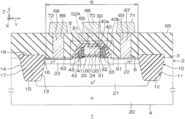
1. A semiconductor device, comprising:
a semiconductor layer having a main surface;
a first conductive type well region formed on a surface portion of the main surface of the semiconductor layer;
a second conductive type source region formed on a surface portion of the well region;
a second conductive type drain region formed on the surface portion of the well region at an interval from the source region;
a planar gate structure that is formed on the main surface of the semiconductor layer so as to face a first conductive type channel region disposed between the source region and the drain region, and includes a gate insulating film formed on the main surface of the semiconductor layer and a gate electrode formed on the gate insulating film;
a memory structure disposed adjacent to a lateral side of the planar gate structure, and including an insulating film formed on the channel region and a charge storage film facing the channel region with the insulating film interposed between the charge storage film and the channel region;
a covering insulating film that covers the planar gate structure and the memory structure; and
an interlayer insulating film that covers the covering insulating film,
wherein the covering insulating film is in contact with the source region and the drain region,
wherein the covering insulating film is in contact with the gate electrode, and
wherein the interlayer insulating film is in contact with the covering insulating film in both a direction in which the gate insulating film, the gate electrode, and the covering insulating film are stacked, and a direction in which the memory structure is disposed adjacent to the lateral side of the planar gate structure.
|