| CPC H10B 12/315 (2023.02) [G11C 11/4085 (2013.01); G11C 11/4091 (2013.01); G11C 11/4097 (2013.01); H01L 21/02565 (2013.01); H01L 29/66969 (2013.01); H01L 29/7869 (2013.01); H10B 12/0335 (2023.02); H10B 12/05 (2023.02); H10B 12/50 (2023.02)] | 15 Claims |

|
1. A semiconductor device comprising:
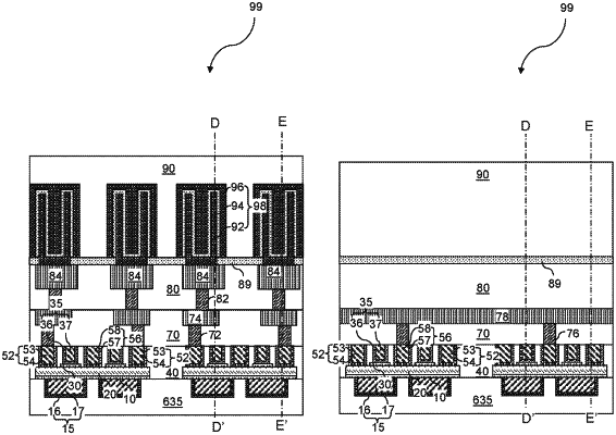
a first thin film transistor and a second thin film transistor comprising a semiconducting metal oxide plate located over a substrate as a continuous material portion, and a set of electrode structures located on the semiconducting metal oxide plate and comprising, from one side to another along a first horizontal direction, a first source electrode, a first gate electrode, a drain electrode, a second gate electrode, and a second source electrode, wherein the first gate electrode and the second gate electrode are spaced from the semiconducting metal oxide plate by a first gate dielectric and a second gate dielectric, respectively, wherein a first portion of the semiconducting metal oxide plate laterally extending between the first source electrode and the drain electrode comprises a first semiconductor channel, and wherein a second portion of the semiconducting metal oxide plate laterally extending between the second source electrode and the drain electrode comprises a second semiconductor channel;
a bit line overlying the semiconducting metal oxide plate, electrically connected to the drain electrode, and laterally extending along the first horizontal direction;
a first capacitor structure comprising a first conductive node that is electrically connected to the first source electrode; and
a second capacitor structure comprising a second conductive node that is electrically connected to the second source electrode,
wherein:
the semiconducting metal oxide plate and each of the first source electrode, the first gate electrode, the drain electrode, the second gate electrode, and the second source electrode are located within a TFT-level dielectric material layer;
each of the first source electrode, the first gate electrode, the drain electrode, the second gate electrode, and the second source electrode comprises a respective horizontal top surface that is located within a horizontal plane including a top surface of the TFT-level dielectric material layer;
each of the first source electrode, the first gate electrode, the drain electrode, the second gate electrode, and the second source electrode comprises a respective horizontal bottom surface, the respective horizontal top surface, and straight sidewalls that vertically extend from a periphery of the respective bottom to surface to a periphery of the respective top surface; and
all of the straight sidewalls of the first source electrode, the first gate electrode, the drain electrode, the second gate electrode, and the second source electrode are in direct contact with the TFT-level dielectric material layer.
|