| CPC H04R 1/1041 (2013.01) [H02J 7/0044 (2013.01); H04R 1/1016 (2013.01); H04R 2420/07 (2013.01)] | 12 Claims |
|
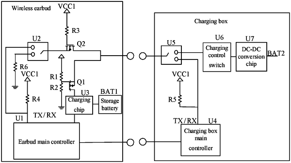
1. A wireless earbud, comprising:
a charging port configured to be connected to an earbud charging voltage and receive/send a communication signal;
a communication switching circuit comprising:
a first input/output terminal connected to the charging port; and
a second input/output terminal; wherein:
the communication switching circuit is configured to switch to an off state when the charging port is connected to the earbud charging voltage, and switch to an on state when the charging port is connected to the communication signal;
a communication on-off circuit connected to the second input/output terminal of the communication switching circuit; and
an earbud control circuit configured to perform box entry detection on the wireless earbud and generate a corresponding detection signal to control the communication switching circuit to turn on/off an electrical connection between the earbud control circuit and the communication on-off circuit according to the detection signal;
the communication switching circuit further comprises:
a second MOS transistor, a source of the second MOS transistor being the second input/output terminal of the communication switching circuit, and a drain of the second MOS transistor being the first input/output terminal of the communication switching circuit; and
a first pull-up resistor, a first terminal of the first pull-up resistor being connected to a first DC power supply, and a second terminal of the first pull-up resistor being connected to a gate of the second MOS transistor.
|