| CPC H03K 5/134 (2014.07) [H03K 5/131 (2013.01); H03K 2005/00071 (2013.01); H03K 2005/00221 (2013.01)] | 20 Claims |
|
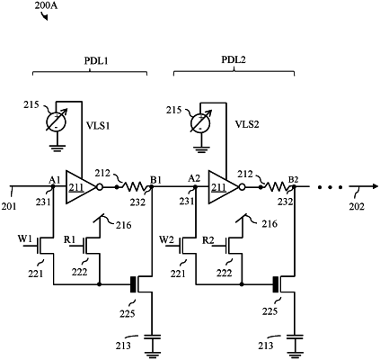
1. A structure comprising:
an input node;
an output node;
an inverter connected between the input node and the output node;
a threshold voltage-programmable field effect transistor;
a capacitor electrically connectable to the output node through the threshold voltage-programmable field effect transistor;
a first access device connected between the input node and a gate structure of the threshold voltage-programmable field effect transistor and controlled by a program mode control signal; and
a second access device connected between a power supply and the gate structure of the threshold voltage-programmable field effect transistor and controlled by a delay mode control signal.
|