| CPC H02M 7/003 (2013.01) [B64D 27/24 (2013.01); H02M 1/08 (2013.01); H02M 7/537 (2013.01); H05K 1/0277 (2013.01); H05K 7/209 (2013.01)] | 18 Claims |
|
1. A power electronics converter comprising:
a multi-layer planar carrier substrate defining an x-y direction parallel to a planar surface of the multi-layer planar carrier substrate and a z-direction perpendicular to the x-y direction, the multi-layer planar carrier substrate comprising a plurality of electrically conductive layers extending in the x-y direction and at least one electrical connection extending in the z-direction;
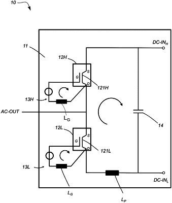
a converter commutation cell comprising a power circuit and a gate driver circuit, the power circuit comprising a power semiconductor switching element and a capacitor, wherein the power semiconductor switching element is comprised in a power semiconductor prepackage, the power semiconductor prepackage comprising one or more power semiconductor switching elements embedded in a solid insulating material, and an electrical connection extending in the z-direction from a terminal of each power semiconductor switching element of the one or more power semiconductor switching elements through the solid insulating material to an electrical connection side of the power semiconductor prepackage, one or more terminals of each power semiconductor switching element of the one or more power semiconductor switching elements of the power semiconductor prepackage being connected to at least one electrically conductive layer of the plurality of electrically conductive layers of the multi-layer planar carrier substrate at the electrical connection side of the power semiconductor prepackage;
a heat sink arranged to remove heat from the power semiconductor prepackage, the heat sink being spaced apart in the z-direction from a heat removal side of the power semiconductor prepackage so as to define a gap between the heat removal side of the power semiconductor prepackage and a thermal connection side of the heat sink;
a thermal interface layer arranged between the heat removal side of the power semiconductor prepackage and the heat sink; and
an electrical isolation layer arranged between the one or more power semiconductor switching elements of the power semiconductor prepackage and the heat sink,
wherein a converter parameter β is greater than or equal to 5 MVW/m2K, where the converter parameter β is a product of a thermal conductivity of the thermal interface layer and a breakdown electric field strength of the electrical isolation layer.
|