| CPC H01L 29/7371 (2013.01) [H01L 29/0821 (2013.01); H01L 29/1004 (2013.01); H01L 29/41708 (2013.01); H01L 29/42304 (2013.01); H01L 29/66234 (2013.01)] | 18 Claims |
|
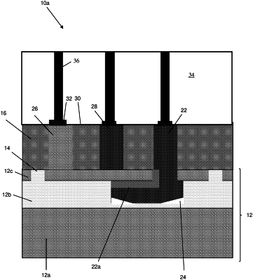
1. A structure comprising:
an intrinsic base region comprising semiconductor-on-insulator material;
a collector region confined within an insulator layer beneath the semiconductor-on-insulator material;
an emitter region above the intrinsic base region;
an extrinsic base region above the intrinsic base region; and
sidewall spacers separating the extrinsic base region from the emitter region, and a collector contact region extending vertically upwards from the collector region.
|