| CPC H01L 29/66545 (2013.01) [H01L 29/0847 (2013.01); H01L 29/161 (2013.01); H01L 29/1608 (2013.01); H01L 29/7851 (2013.01)] | 20 Claims |

|
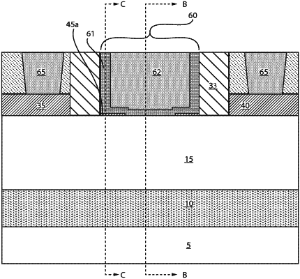
1. A semiconductor device comprising:
a fin structure;
a channel epitaxial wrap around layer present on each end of a channel portion of the fin structure, wherein the channel epitaxial wrap around layer is a continuous and conformal layer;
a gate structure including a gate dielectric having end portions in direct contact with the channel epitaxial wrap around layer at said each end of the channel portion, and a middle portion of the gate dielectric is in direct contact with the fin structure at a portion between said each end of the channel portion;
source and drain regions on portions of the fin structure that are on opposing sides of the channel portion; and
spacers separating the gate structure from source and drain regions.
|