| CPC H01L 29/66242 (2013.01) [H01L 29/165 (2013.01); H01L 29/737 (2013.01)] | 20 Claims |
|
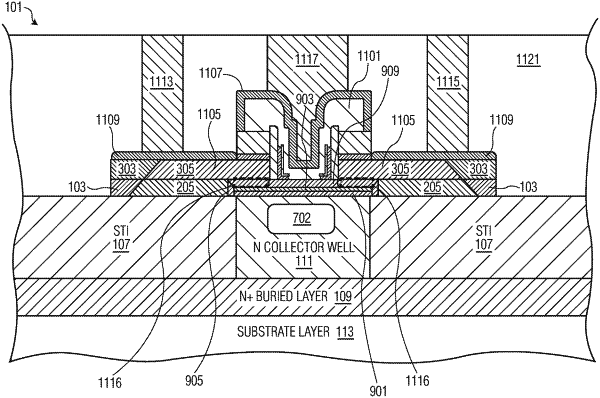
1. A method for forming a semiconductor die including a transistor, the method comprising:
on a wafer including a first semiconductor layer and a second semiconductor layer located on the first semiconductor layer, forming a first opening in the second semiconductor layer at a first area of the wafer to expose the first semiconductor layer, the first semiconductor layer being located directly over a region of monocrystalline semiconductor material in the first area;
after the forming the first opening, removing a portion of the first semiconductor layer to form a cavity with an etch chemistry that is selective with respect to semiconductor material of the first semiconductor layer in the first area and selective to semiconductor material of the second semiconductor layer in the first area, wherein the removing the portion exposes at least a portion of the region of monocrystalline semiconductor material in the first area and exposes an underside portion of the second semiconductor layer laterally adjacent to the first opening;
selectively growing monocrystalline semiconductor material in the cavity, the selectively grown monocrystalline semiconductor material contacting the region of monocrystalline semiconductor material in the first area and a portion of an underside portion of the second semiconductor layer;
forming an emitter of a transistor, the emitter including at least a portion located in the first area;
separating the wafer into a plurality of die including a first die, wherein the first die includes the transistor, the transistor including an intrinsic base region located in the selectively grown monocrystalline semiconductor material and a collector including a portion located in the region of monocrystalline semiconductor material in the first area.
|