| CPC H01L 29/0653 (2013.01) [H01L 29/4236 (2013.01); H01L 29/66704 (2013.01); H01L 29/7825 (2013.01); H01L 29/7835 (2013.01)] | 20 Claims |
|
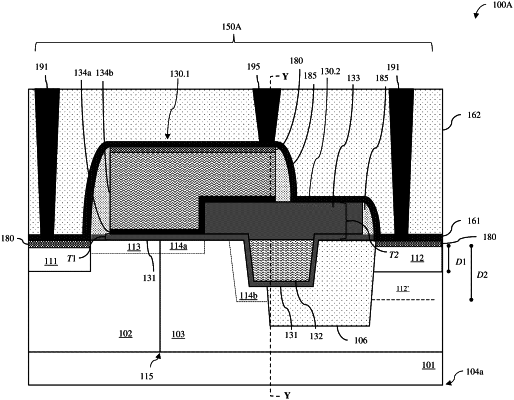
1. A semiconductor structure comprising:
a semiconductor layer; and
a transistor comprising:
a first well in the semiconductor layer and having a first type conductivity;
a second well in the semiconductor layer positioned laterally adjacent to the first well and having a second type conductivity that is different from the first type conductivity;
a trench gate structure in the second well and physically separated from a junction between the first well and the second well; and
a primary gate structure on the semiconductor layer traversing the junction,
wherein gate conductor materials of the trench gate structure and the primary gate structure are physically separated by a gate dielectric material.
|