| CPC H01L 24/05 (2013.01) [G01N 27/225 (2013.01); H01L 24/03 (2013.01); H01L 24/06 (2013.01); H01L 2224/02206 (2013.01); H01L 2224/0382 (2013.01)] | 10 Claims |
|
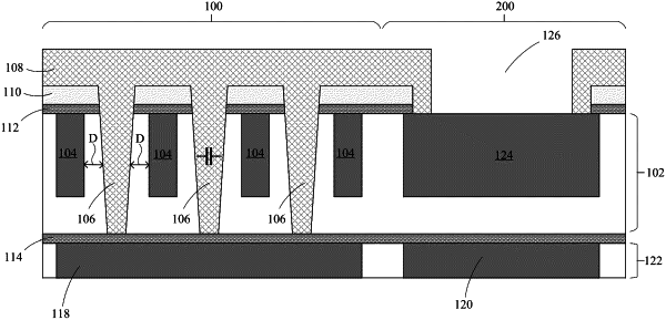
1. A method of forming a semiconductor device, the method comprising:
forming a plurality of electrodes and a bond pad in a dielectric region, wherein the plurality of electrodes is located in a first device region and the bond pad is located in a second device region;
forming a passivation layer on each electrode in the plurality of electrodes and the bond pad;
forming a barrier layer on the passivation layer;
forming a plurality of trenches that extend through the barrier layer and into the dielectric region, the forming of the trenches simultaneously exposing an upper surface of the bond pad; and
forming a moisture sensitive dielectric layer on the barrier layer, wherein the forming of the moisture sensitive dielectric layer also fills the trenches to form a plurality of projections, each projection being formed between two electrodes in the plurality of electrodes.
|