| CPC H01L 23/562 (2013.01) [H01L 23/3121 (2013.01); H01L 23/49861 (2013.01); H01L 2924/3511 (2013.01)] | 20 Claims |
|
1. A microelectronic device package, comprising:
a substrate;
one or more microelectronic devices positioned over the substrate;
at least one warpage control layer; and
an encapsulant material positioned between the at least one warpage control layer and the one or more microelectronic devices;
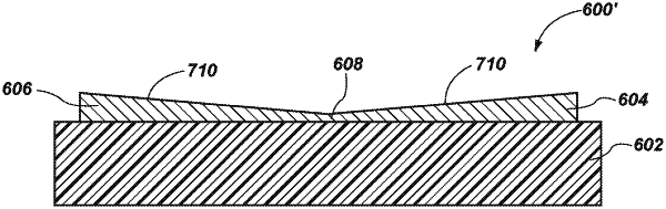
wherein the at least one warpage control layer is coupled to the encapsulant material, the at least one warpage control layer having a first region having a first material having a first coefficient of thermal expansion and a first thickness and a second region having a second material having a second coefficient of thermal expansion different from the first coefficient of thermal expansion and a second thickness greater than the first thickness of the first region.
|