| CPC H01L 23/5226 (2013.01) [G06F 30/394 (2020.01)] | 20 Claims |

|
1. A method of manufacturing a semiconductor device, the method comprising:
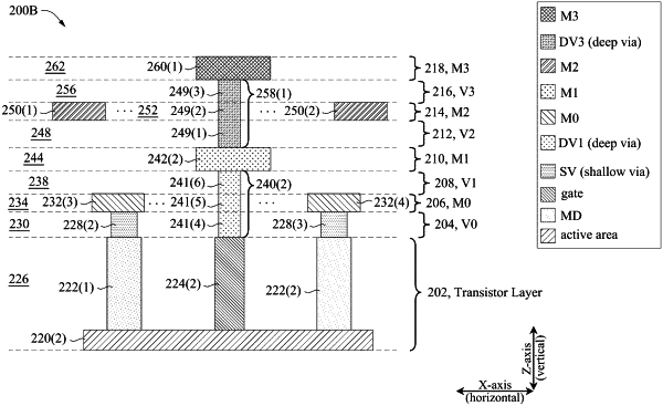
forming via structures in a first via layer over a transistor layer, the forming the via structures in the first via layer including:
forming a first via structure in the first via layer, the first via structure being included in a first deep via arrangement;
forming conductive segments in a first metallization layer over the first via layer, the forming the conductive segments in the first metallization layer including:
forming M_1st routing segments at least a majority of which, relative to a first direction, have corresponding long axes with lengths which at least equal if not exceed a first permissible minimum value for routing segments in the first metallization layer; and
forming an M_1st interconnection segment having a long axis which is less than the first permissible minimum value, the M_1st interconnection segment being included in the first deep via arrangement.
|