US 11,854,933 B2
Thermally conductive wafer layer
Benjamin Stassen Cook, Santa Clara, CA (US); Nazila Dadvand, Santa Clara, CA (US); Archana Venugopal, Mountain View, CA (US); and Daniel Lee Revier, Garland, TX (US)
Assigned to TEXAS INSTRUMENTS INCORPORATED, Dallas, TX (US)
Filed by Texas Instruments Incorporated, Dallas, TX (US)
Filed on Dec. 30, 2020, as Appl. No. 17/138,541.
Prior Publication US 2022/0208640 A1, Jun. 30, 2022
Int. Cl. H01L 23/373 (2006.01); H01L 23/532 (2006.01); H01L 21/683 (2006.01); H01L 21/3205 (2006.01); H01L 21/78 (2006.01)
CPC H01L 23/373 (2013.01) [H01L 21/32051 (2013.01); H01L 21/6835 (2013.01); H01L 21/78 (2013.01); H01L 23/53209 (2013.01)] 17 Claims
OG exemplary drawing
 
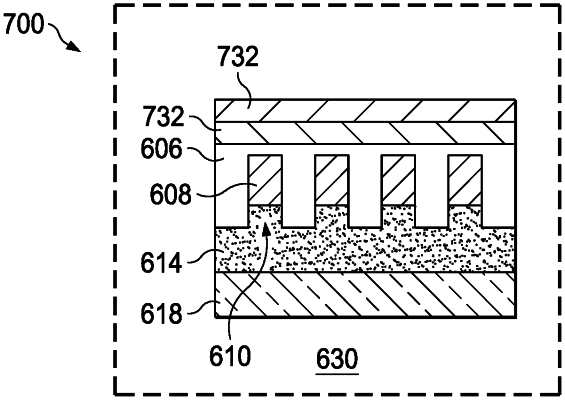
1. An integrated circuit, comprising:
a semiconductor substrate having opposite first and second surfaces, the first surface having a patterned region;
circuitry in the patterned region of the first surface;
a metallic layer on the second surface; and
a carbon layer on the metallic layer.