| CPC H01L 23/3171 (2013.01) [H01L 21/0217 (2013.01); H01L 21/02126 (2013.01); H01L 21/02129 (2013.01); H01L 21/02164 (2013.01); H01L 21/283 (2013.01); H01L 21/28247 (2013.01); H01L 21/3081 (2013.01); H01L 21/56 (2013.01); H01L 23/29 (2013.01); H01L 23/3192 (2013.01); H01L 27/0629 (2013.01); H01L 29/0619 (2013.01); H01L 29/1066 (2013.01); H01L 29/47 (2013.01); H01L 29/66674 (2013.01); H01L 29/66901 (2013.01); H01L 29/70 (2013.01); H01L 29/7397 (2013.01); H01L 29/7801 (2013.01); H01L 29/7811 (2013.01); H01L 29/7813 (2013.01); H01L 29/808 (2013.01); H01L 29/8083 (2013.01); H01L 29/8611 (2013.01); H01L 29/872 (2013.01); H01L 29/0615 (2013.01); H01L 29/0638 (2013.01); H01L 29/0661 (2013.01); H01L 29/4236 (2013.01); H01L 2224/05567 (2013.01); H01L 2224/05624 (2013.01); H01L 2224/05647 (2013.01); H01L 2224/05666 (2013.01); H01L 2924/1033 (2013.01); H01L 2924/10272 (2013.01); H01L 2924/10329 (2013.01); H01L 2924/10331 (2013.01); H01L 2924/10335 (2013.01); H01L 2924/10346 (2013.01); H01L 2924/10373 (2013.01); H01L 2924/13055 (2013.01); H01L 2924/13062 (2013.01); H01L 2924/13091 (2013.01)] | 20 Claims |
|
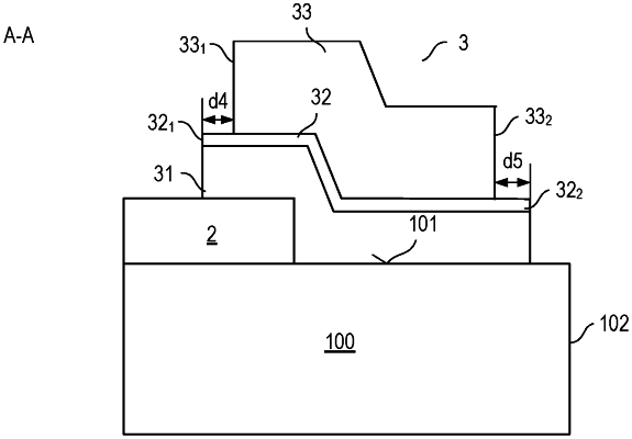
1. A semiconductor device, comprising:
a semiconductor body comprising a first surface and an edge surface laterally terminating the first surface;
a contact electrode formed above the first surface and comprising an outer edge side that faces and is laterally spaced apart from the edge surface; and
a passivation layer section covering the outer edge side of the contact electrode,
wherein the passivation layer section is a multi-layer stack comprising a first layer, a second layer, and a third layer, each of the first, second and third layers being formed from different electrically insulating materials,
wherein the first layer directly contacts the contact electrode,
wherein the second layer is formed directly on the first layer,
wherein the third layer is formed directly on the second layer,
wherein each of the first, second and third layers comprise outer edge sides facing the edge surface of the semiconductor body and inner edge sides opposite from the outer edge sides,
wherein the outer edge side of the contact electrode extends along a first plane that is transverse to the first surface,
wherein the first plane is disposed laterally between the inner edge sides and the outer edge sides of each of the first, second and third layers,
wherein a separation distance between the inner edge side of the third layer and the first plane is different than a separation distance between the inner edge side of the second layer and the first plane,
wherein a separation distance between the outer edge side of the third layer and the first plane is different than a separation distance between the outer edge side of the second layer and the first plane.
|